| CPC H10B 63/80 (2023.02) [H10B 63/24 (2023.02); H10N 70/063 (2023.02); H10N 70/231 (2023.02)] | 20 Claims |
|
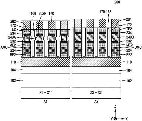
1. A resistive memory device comprising:
a plurality of first conductive lines extending in a first horizontal direction in a first area and a second area on a substrate, the first horizontal direction being parallel to the substrate;
a plurality of second conductive lines extending in a second horizontal direction crossing the first horizontal direction in the first area and the second area, the plurality of second conductive lines being apart from the plurality of first conductive lines in a vertical direction, the vertical direction being perpendicular to the substrate; and
a plurality of memory cells connected to the first conductive lines and the second conductive lines at a plurality of intersections between the plurality of first conductive lines and the plurality of second conductive lines in the first area and the second area,
wherein the plurality of memory cells comprise an active memory cell in the first area and a dummy memory cell in the second area, the active memory cell including a first resistive memory pattern having a first width in a horizontal direction, and the dummy memory cell including a second resistive memory pattern having a second width in the horizontal direction, and the first width is less than the second width.
|