| CPC H10B 53/30 (2023.02) [G11C 11/2255 (2013.01); H10B 51/20 (2023.02); H10B 51/30 (2023.02); H10B 51/40 (2023.02); H10B 53/20 (2023.02); H10B 53/40 (2023.02)] | 15 Claims |
|
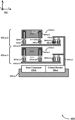
1. A memory device, comprising:
a column decoder of a memory die;
a first memory array at a first level above a substrate of the memory die, the first memory array comprising a first plurality of digit lines each operable to couple with the column decoder based at least in part on activating a respective first transistor at the first level; and
a second memory array at a second level above the substrate of the memory die, the second memory array comprising a second plurality of digit lines each operable to couple with the column decoder based at least in part on activating a respective second transistor at the second level.
|