| CPC H10B 43/27 (2023.02) [H10B 12/50 (2023.02); H10B 43/40 (2023.02)] | 7 Claims |
|
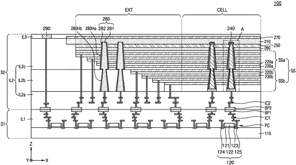
1. A nonvolatile memory device comprising:
a first structure, the first structure including a first substrate, a peripheral circuit on the first substrate, a first insulating structure on the first substrate and the peripheral circuit, a plurality of first bonding pads on the first insulating structure, and a first interconnect structure in the first insulating structure and connected to the peripheral circuit and the plurality of first bonding pads; and
a second structure bonded to the first structure, the second structure including a low-resistance conductive layer, a common source line layer on the low-resistance conductive layer, a stack structure including a plurality of gate layers and a plurality of interlayer insulating layers alternately stacked above the common source line layer, a plurality of channel structures passing through a cell region of the stack structure and contacting the common source line layer, a dummy channel structure passing through a step region of the stack structure and contacting the common source line layer, a second insulating structure including a first portion, a second portion, and a third portion, the second insulating structure on the stack structure, a plurality of second bonding pads on the second insulating structure, a second interconnect structure in the second insulating structure, a lower conductive layer between the common source line layer and the stack structure, and a lower support layer between the stack structure and the lower conductive layer, wherein
the second interconnect structure being connected to the plurality of gate layers, the plurality of channel structures, the dummy channel structure, and the plurality of second bonding pads,
the plurality of second bonding pads contacting the plurality of first bonding pads, respectively,
the step region of the stack structure being on one side of the cell region of the stack structure and having a stepped shape,
each of the plurality of channel structures comprises a channel layer and a gate insulating layer,
the gate insulating layer is between the channel layer and the cell region of the stack structure,
the lower conductive layer passes through the gate insulating layer and contacts the channel layer, and
the second interconnect structure is connected to the dummy channel structure in an interface between the first portion and the second portion of the second insulating structure.
|