| CPC H10B 12/485 (2023.02) [H01L 25/0657 (2013.01); H10B 12/0335 (2023.02); H10B 12/315 (2023.02); H10B 12/482 (2023.02); H10B 12/488 (2023.02); H10B 12/50 (2023.02); H10B 80/00 (2023.02)] | 17 Claims |
|
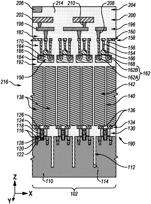
1. A method of forming a microelectronic device, comprising:
forming a microelectronic device structure comprising memory cells, digit lines, word lines, and at least one isolation material covering and surrounding the memory cells, the digit lines, and the word lines;
forming an additional microelectronic device structure comprising control logic devices and at least one additional isolation material covering and surrounding the control logic devices;
attaching the additional microelectronic device structure to the microelectronic device structure to form an assembly, the control logic devices overlying the memory cells within the assembly, transistors of the control logic devices positioned relatively more proximate to the memory cells than are conductive routing structures of the control logic devices coupled to the transistors; and
forming contact structures extending through the at least one isolation material and the at least one additional isolation material after forming the assembly, some of the contact structures coupled to some of the digit lines and some of the control logic devices, and some other of the contact structures coupled to some of the word lines and some other of the control logic devices.
|