| CPC H10B 12/482 (2023.02) [H10B 12/312 (2023.02); H10B 12/488 (2023.02)] | 15 Claims |
|
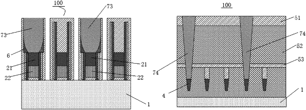
12. A semiconductor device, comprising:
a substrate;
a word line structure formed in the substrate;
a bit line structure formed on the substrate and traversing the word line structure;
a supporting structure formed on the substrate; wherein the supporting structure comprises a bit line supporting layer and a word line supporting layer, the bit line supporting layer comprising a first oxide layer and a first nitride layer; wherein the bit line structure is formed in the first nitride layer, and the first oxide layer is formed on both sides of the bit line structure and in the first nitride layer; wherein the word line supporting layer comprises a second nitride layer, a second oxide layer and a third nitride layer that are stacked, and the second oxide layer is formed between the second nitride layer and the third nitride layer, wherein a first via is formed in the bit line supporting layer to expose the bit line structure, and a second via is formed in the word line supporting layer to expose the word line structure; and
a polymer layer formed in the first via and formed on part of a sidewall of the first via above the first oxide layer.
|