| CPC H10B 10/18 (2023.02) [G11C 5/14 (2013.01); H10B 10/12 (2023.02); G11C 11/412 (2013.01)] | 20 Claims |
|
1. A semiconductor memory device, comprising:
a plurality of memory cells on a substrate, each of the plurality of memory cells including an access transistor and a pull-down transistor;
a first line layer on the memory cells, the first line layer including a power line, a first lower landing pad, and a second lower landing pad;
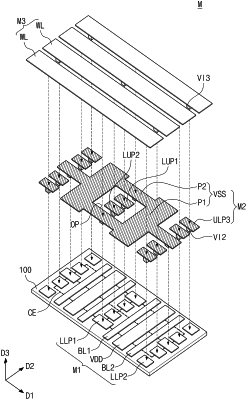
a second line layer on the first line layer, the second line layer including a ground line (52) having an opening, an upper landing pad (50) in the opening, and vias provided below the ground line and the upper landing pad, the opening surrounding the upper landing pad when viewed in a plan view, the ground line including a pair of first segments and a pair of second segments that define the opening, each of the first segments extending in a first direction and having a first width in a second direction intersecting the first direction, each of the second segments extending in the second direction and having a second width in the first direction; and
a third line layer including a word line on the second line layer,
wherein the ground line is electrically connected through the first lower landing pad to a terminal of the pull-down transistor, and
wherein the word line is electrically connected through the upper landing pad and the second lower landing pad to a terminal of the access transistor,
wherein the power line included in the first line layer is under a corresponding one of the first segments of the ground line included in the second line layer, and the power line vertically overlaps the corresponding one of the first segments,
wherein both sidewalls of the power line vertically overlap the corresponding one of the first segments such that a third width of the power line (in the second direction) is less than or equal to the first width,
wherein the vias below the ground line are connected only to the second segments and not to the first segments.
|