US 11,930,628 B2
Semiconductor device and manufacturing method thereof
Yu-I Shih, Taichung (TW); and Ren-Hua Guo, Taichung (TW)
Assigned to TAIWAN SEMICONDUCTOR MANUFACTURING CO., LTD., Hsinchu (TW)
Filed by TAIWAN SEMICONDUCTOR MANUFACTURING CO., LTD., Hsinchu (TW)
Filed on Apr. 3, 2023, as Appl. No. 18/295,249.
Application 18/295,249 is a continuation of application No. 17/394,914, filed on Aug. 5, 2021, granted, now 11,621,268.
Application 17/394,914 is a continuation of application No. 16/259,824, filed on Jan. 28, 2019, granted, now 11,088,150, issued on Aug. 10, 2021.
Prior Publication US 2023/0247818 A1, Aug. 3, 2023
Int. Cl. H10B 10/00 (2023.01); H01L 21/02 (2006.01); H01L 21/3065 (2006.01); H01L 21/8238 (2006.01); H01L 29/04 (2006.01); H01L 29/165 (2006.01); H01L 29/66 (2006.01); H01L 29/78 (2006.01)
CPC H10B 10/12 (2023.02) [H01L 21/02293 (2013.01); H01L 21/3065 (2013.01); H01L 21/823821 (2013.01); H01L 29/045 (2013.01); H01L 29/165 (2013.01); H01L 29/66795 (2013.01); H01L 29/7853 (2013.01); H01L 29/7854 (2013.01)] 20 Claims
OG exemplary drawing
 
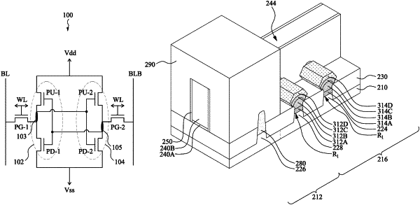
1. A device, comprising:
a substrate;
a pull-down transistor over the substrate;
a pass-gate transistor over the substrate; and
a pull-up transistor over the substrate, comprising:
a first gate structure; and
first source/drain epitaxy structures on opposite sides of the first gate structure, wherein each of the first source/drain epitaxy structures comprises a first epitaxy layer and a second epitaxy layer over the first epitaxy layer, wherein a germanium concentration of the first epitaxy layer is higher than a germanium concentration of the second epitaxy layer.