| CPC H05K 1/0281 (2013.01) [H01R 12/79 (2013.01); H05K 1/148 (2013.01); H05K 1/189 (2013.01); H05K 5/0017 (2013.01); H05K 2201/093 (2013.01); H05K 2201/10151 (2013.01); H05K 2201/10189 (2013.01); H05K 2201/2009 (2013.01)] | 18 Claims |
|
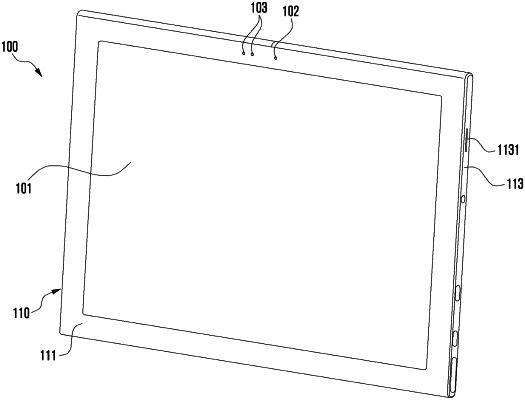
1. An electronic device comprising:
a housing;
a first printed circuit board disposed in an internal space of the housing;
a second printed circuit board disposed to be spaced apart from the first printed circuit board; and
a flexible printed circuit board that electrically connects the first printed circuit board and the second printed circuit board, the flexible printed circuit board including a connection part connected to the second printed circuit board, and a linkage part extended from the connection part, the linkage part including a bending portion being at least partially bendable, the flexible printed circuit board further including:
a dielectric substrate,
a first conductive layer disposed on a first surface of the dielectric substrate,
a first cover layer disposed on the first conductive layer,
a second conductive layer disposed on a second surface opposite to the first surface of the dielectric substrate,
a second cover layer disposed on the second conductive layer,
a plurality of first conductive terminals, in the connection part, exposed through the first cover layer and electrically connected to the first conductive layer, and
a plurality of second conductive terminals, in the connection part, exposed through the first cover layer, electrically connected to the first conductive layer, and disposed at a greater distance from the bending portion than the plurality of first conductive terminals,
wherein the first conductive layer includes, at the bending portion, a cutoff portion at which the first conductive layer is electrically disconnected,
wherein the plurality of second conductive terminals are electrically connected to the second conductive layer, in the connection part, through at least one conductive via formed through the dielectric substrate, and
wherein the cutoff portion at least partially overlaps the connection part and the bending portion when the flexible printed circuit board is viewed from above.
|