| CPC H05H 1/2425 (2021.05) | 15 Claims |
|
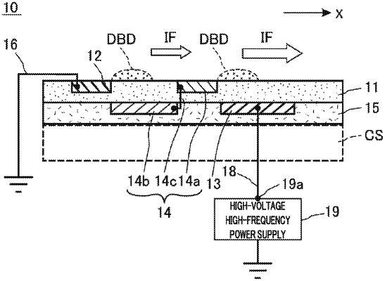
1. A plasma actuator that allows an induced flow to be generated, the plasma actuator comprising:
a dielectric layer;
a first electrode provided on a front surface of the dielectric layer;
a second electrode provided on a side of a back surface of the dielectric layer in one direction from the first electrode;
a floating conductor pair provided between the first electrode and the second electrode and including a front surface conductor disposed on the front surface of the dielectric layer and a back surface conductor disposed on the side of the back surface of the dielectric layer, wherein the front surface conductor and the back surface conductor are electrically connected to each other and are electrically insulated from the first electrode and the second electrode and the back surface conductor and the front surface conductor are disposed in this order in the one direction from the first electrode in plan view; and
a power supply connected to the first electrode and the second electrode, wherein
the plasma actuator allows the induced flow to be produced along the front surface of the dielectric layer in the one direction from the first electrode by applying a high-frequency high voltage between the first electrode and the second electrode by the power supply to thereby generate dielectric barrier discharge on the front surface between the first electrode and the back surface conductor and on the front surface between the front surface conductor and the second electrode.
|