| CPC H03M 13/118 (2013.01) [H03M 13/1575 (2013.01); H03M 13/611 (2013.01); H03M 13/1174 (2013.01); H03M 13/658 (2013.01)] | 2 Claims |
|
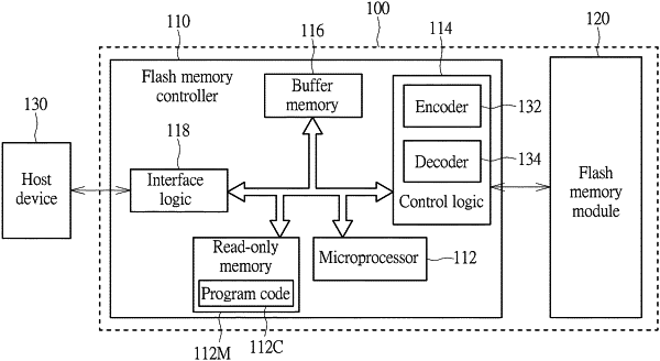
1. A flash memory controller, arranged to access a flash memory module, and comprising:
a memory, arranged to store a program code;
a microprocessor, arranged to execute the program code to control access of the flash memory module; and
an encoder, arranged to encode multiple data blocks to obtain multiple parity blocks, wherein the encoder comprises:
a first barrel shifter module, arranged to process the multiple data blocks to generate multiple partial parity blocks, wherein the multiple partial parity blocks comprise a first part and a second part, generation time of the first part is earlier than generation time of the second part, and a number of partial parity blocks comprised in the first part is less than a number of partial parity blocks comprised in the second part;
an adjustment circuit, arranged to adjust the second part of the multiple partial parity blocks according to the first part, to generate an adjusted second part;
a circulant convolution calculation circuit, coupled to the adjustment circuit, and arranged to perform a circulant convolution operation upon the adjusted second part, to generate a second part parity block; and
a calculation circuit, coupled to the circulant convolution calculation circuit, and arranged to generate a first part parity block according to the second part parity block;
wherein the first part parity block and the second part parity block act as multiple parity blocks that are generated by the encoder for the multiple data blocks, and the multiple data blocks and the multiple parity blocks are written into a flash memory;
wherein both of the multiple data blocks and the multiple parity blocks are multiplied by a parity-check matrix, to determine whether the multiple parity blocks are correct only if the multiple parity blocks are determined to be correct, the multiple data blocks and the multiple parity blocks are written into the flash memory;
wherein each submatrix in the first column and the first row of the parity-check matrix is an identity matrix;
wherein the flash memory controller further comprises a decoder, and the decoder comprises:
a second barrel shifter module and multiple accumulation circuits, arranged to process multiple read data blocks read from the flash memory module, to generate multiple decoding syndromes, wherein a number of barrel shifters comprises in the second barrel shifter module is less than a number of the multiple accumulation circuits, and the number of barrel shifters comprises in the second barrel shifter module is less than a number of the multiple decoding syndromes.
|