| CPC H03H 9/1071 (2013.01) [H03H 3/02 (2013.01); H03H 3/08 (2013.01); H03H 9/02086 (2013.01); H03H 9/02913 (2013.01); H03H 9/1014 (2013.01); H10N 30/02 (2023.02); H10N 30/06 (2023.02); H10N 30/875 (2023.02); H10N 30/883 (2023.02)] | 6 Claims |
|
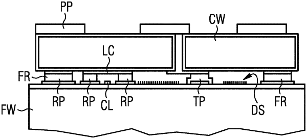
1. A wafer level package, comprising:
a functional wafer with a first surface;
device structures connected to device pads arranged on the first surface;
a cap wafer having an inner surface and an outer surface, the inner surface being bonded to the first surface of the functional wafer;
a frame structure surrounding the device structures and being arranged between the functional wafer and the cap wafer;
connection posts connecting the device pads on the first surface to inner cap pads on the inner surface;
electrically conducting vias guided through the cap wafer connecting the inner cap pads on the inner surface and package pads on the outer surface of the cap wafer
a bridging line on the inner surface connecting two of the connection posts; and
a conductor line on the first surface, wherein an air gap exists between the bridging line and the conductor line such that the bridging line and the conductor line form a contactless line crossing.
|