| CPC H03F 1/303 (2013.01) [H03F 1/52 (2013.01); H03F 3/005 (2013.01); H03F 3/45632 (2013.01)] | 14 Claims |
|
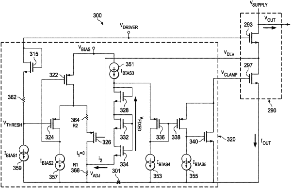
1. An output stage, comprising:
a first metal oxide semiconductor (MOS) device having a first gate, a first drain, and a first source; and
a current limit circuit comprising
a second MOS device having a second gate, a second drain, and a second source, the second gate being coupled to a drain of the first MOS device;
a resistor coupled between the second drain and a ground;
a third MOS device having a third gate, a third drain, and a third source, the third gate being coupled to a first voltage source, the third source being coupled to the second source, and the third drain being coupled to a first current source,
the second MOS device operating in an OFF mode responsive to a drain voltage of the first MOS device being greater than the first voltage source, and the second MOS device operating in an ON mode responsive to the drain voltage of the first MOS device being less than the first voltage source;
a plurality of series-connected MOS devices, wherein a first voltage is generated across the plurality of series-connected MOS devices in response to a biasing current supplied to a drain of one of the plurality of series-connected MOS devices, wherein a source of another of the plurality of series-connected MOS devices is coupled to the resistor; and
a voltage clamp circuit coupled between the drain of the one of the plurality of series-connected MOS devices and the first gate.
|