| CPC H02M 3/07 (2013.01) | 20 Claims |
|
1. A voltage multiplier circuit comprising:
a first input node and a second input node configured to be coupled to a voltage source to receive an input voltage therebetween;
a first output node and a second output node configured to be coupled to an output capacitor to produce an output voltage across the output capacitor;
a first input control node configured to receive a first clock signal and a second input control node configured to receive a second clock signal, the second clock signal being in phase opposition to the first clock signal, wherein the voltage multiplier circuit switches between a first commutation state and a second commutation state as a function of the values of the first clock signal and the second clock signal;
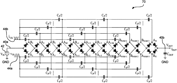
an ordered sequence of intermediate voltage nodes arranged between the first input node and the first output node, the ordered sequence comprising a first ordered sub-sequence of intermediate voltage nodes and a second ordered sub-sequence of intermediate voltage nodes;
a respective capacitor coupled between each odd-numbered intermediate voltage node in the first ordered sub-sequence of the ordered sequence and the first input control node, wherein a first intermediate voltage node in the first ordered sub-sequence is configured to be selectively couplable to the first input node;
a respective capacitor coupled between each even-numbered intermediate voltage node in the first ordered sub-sequence of the ordered sequence and the second input control node;
a respective capacitor coupled between each odd-numbered intermediate voltage node in the second ordered sub-sequence of the ordered sequence and a corresponding odd-numbered intermediate voltage node in the first ordered sub-sequence of the ordered sequence;
a respective capacitor coupled between each even-numbered intermediate voltage node in the second ordered sub-sequence of the ordered sequence and a corresponding even-numbered intermediate voltage node in the first ordered sub-sequence of the ordered sequence; and
a first plurality of selectively conductive electronic components coupled to the intermediate voltage nodes of the ordered sequence, wherein:
in the first commutation state of the voltage multiplier circuit, the first plurality of selectively conductive electronic components is configured to provide electrically-conductive paths between each of the even-numbered intermediate voltage nodes of the ordered sequence and a respective next odd-numbered intermediate voltage node of the ordered sequence, an electrically-conductive path between the first input node and the first intermediate voltage node of the ordered sequence, and an electrically-conductive path between a last intermediate voltage node of the ordered sequence and the first output node, and
in the second commutation state of the voltage multiplier circuit, the first plurality of selectively conductive electronic components is configured to provide electrically-conductive paths between each of the odd-numbered intermediate voltage nodes of the ordered sequence and a respective next even-numbered intermediate voltage node of the ordered sequence.
|