| CPC H01S 5/22 (2013.01) [H01S 5/0234 (2021.01); H01S 5/0237 (2021.01); H01S 5/34333 (2013.01)] | 16 Claims |
|
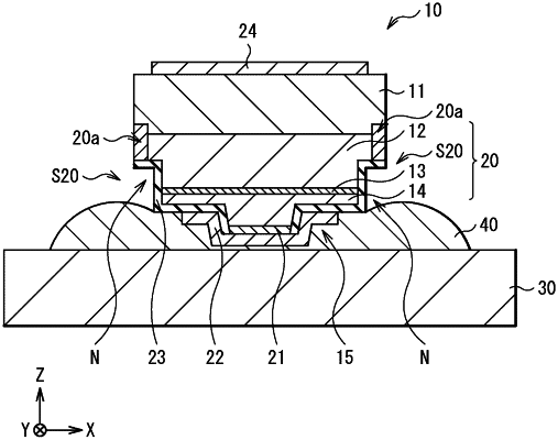
1. A semiconductor light-emitting device, comprising:
a stacked body that includes a first conductive-type semiconductor layer, an active layer, and a second conductive-type semiconductor layer in this order, wherein the stacked body has paired side faces opposed to each other;
a cutout section that is on at least one of the paired side faces of the stacked body, wherein the cutout section has a bottom face where the first conductive-type semiconductor layer is exposed; and
a high-resistance region that is in vicinity of the bottom face of the cutout section and the side face of the stacked body, wherein the high-resistance region has electric resistance higher than electric resistance of the stacked body in a periphery of the high-resistance region.
|