| CPC H01Q 1/243 (2013.01) [H01Q 9/0407 (2013.01); H01Q 9/16 (2013.01); H05K 1/142 (2013.01); H05K 5/0017 (2013.01); H05K 5/0226 (2013.01); H04B 1/40 (2013.01); H05K 2201/09018 (2013.01); H05K 2201/10098 (2013.01); H05K 2201/10128 (2013.01)] | 13 Claims |
|
1. An electronic device comprising:
a housing comprising a first plate, a second plate facing away from the first plate, and a side member surrounding a space between the first plate and the second plate;
a display visible through a portion of the first plate;
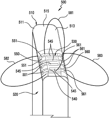
a first printed circuit board comprising a first surface facing the side member, a second surface facing away from the first surface, a first edge located close to the first plate, and a second edge located closer to the second plate than the first edge, the first printed circuit board comprising one or more conductive plates disposed on the first surface;
a second printed circuit board extending from the first edge and bent while forming an obtuse angle with the first surface, the second printed circuit board comprising one or more first conductive patterns facing the side member;
a third printed circuit board extending from the second edge and bent while forming an obtuse angle with the first surface, the third printed circuit board comprising one or more second conductive patterns facing the side member; and
a wireless communication circuit configured to transmit and/or receive signals having a frequency between 3 gigahertz (GHz) and 300 GHz using the one or more conductive plates, the one or more first conductive patterns forming a first signal beam toward the side member, and the one or more second conductive patterns forming a second signal beam toward the side member.
|