| CPC H01L 33/405 (2013.01) [H01L 33/06 (2013.01); H01L 33/12 (2013.01); H01L 33/22 (2013.01); H01L 33/42 (2013.01); H01L 33/46 (2013.01); H01L 33/502 (2013.01); H01L 33/60 (2013.01); H01L 33/62 (2013.01); H01L 2933/0016 (2013.01)] | 20 Claims |
|
1. A semiconductor light emitting device, comprising:
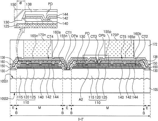
a light-emitting structure including a first conductivity-type semiconductor layer, an active layer, and a second conductivity-type semiconductor layer;
a transparent electrode layer on the second conductivity-type semiconductor layer, the transparent electrode layer being spaced apart from an edge of the second conductivity-type semiconductor layer;
a first insulating layer on the light-emitting structure to cover the transparent electrode layer, the first insulating layer including a plurality of holes connected to the transparent electrode layer;
a reflective electrode layer on the first insulating layer and connected to the transparent electrode layer through the plurality of holes;
a second insulating layer on the first insulating layer to cover the reflective electrode layer, the second insulating layer including at least one first opening and at least one second opening;
a first connection electrode on the second insulating layer and connected to the reflective electrode layer through the at least one first opening;
a second connection electrode on the second insulating layer and connected to the first conductivity-type semiconductor layer through the at least one second opening;
a third insulating layer on the second insulating layer, the third insulating layer including a third opening exposing a portion of the first connection electrode and a fourth opening exposing a portion of the second connection electrode;
a first electrode pad contacting the first connection electrode through the third opening; and
a second electrode pad contacting the second connection electrode through the fourth opening,
wherein each of the first connection electrode and the second connection electrode includes a first electrode layer, a second electrode layer, and a conductive barrier layer between the first electrode layer and the second electrode layer,
wherein the first electrode layer includes an edge region and an internal region surrounded by the edge region, the edge region has a thickness less than a thickness of the internal region, and the second electrode layer has a thickness greater than that of the first electrode layer,
wherein the light-emitting structure includes a recessed region exposing a portion of the first conductivity-type semiconductor layer, and a mesa region surrounded by the recessed region,
wherein at least one of the first connection electrode and the second connection electrode has a first portion covering a side surface of the mesa region of the light-emitting structure, and a second portion covering the exposed portion of the first conductivity-type semiconductor layer at an edge of the light-emitting structure, and
wherein the first portion extends downwardly along the side surface of the mesa region, and the second portion extends in parallel to the exposed portion of the first conductivity-type semiconductor layer.
|