| CPC H01L 31/022425 (2013.01) [H01L 31/05 (2013.01); H01L 31/0543 (2014.12)] | 17 Claims |
|
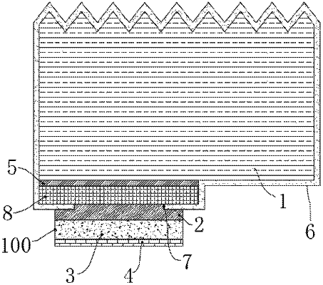
1. A conductive contact structure of a solar cell, the conductive contact structure comprising:
a substrate;
a semiconductor region; and
an electrode;
wherein:
the semiconductor region is disposed on or in the substrate;
the electrode is disposed on the semiconductor region;
the electrode comprises:
a seed layer in contact with the semiconductor region, wherein the seed layer comprises an alloy material, which comprises a first component and a second component, wherein:
the first component is Al in an amount greater than or equal to 70 wt. % of the seed layer; and
the second component comprises any one or more of Mo, Ti, and W in an amount less than or equal to 30 wt. % of the seed layer; and
a conductive layer comprising Cu disposed above the seed layer.
|