| CPC H01L 29/7869 (2013.01) [C23C 14/0676 (2013.01); C23C 14/08 (2013.01); C23C 14/086 (2013.01); C23C 14/3414 (2013.01); H01L 21/02554 (2013.01); H01L 21/02565 (2013.01); H01L 21/02631 (2013.01); H01L 29/24 (2013.01); H01L 29/4908 (2013.01); H01L 29/518 (2013.01); H01L 29/66969 (2013.01)] | 18 Claims |
|
1. A transistor comprising:
an oxide semiconductor layer; and
a gate insulating film in contact with the oxide semiconductor layer,
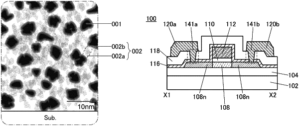
wherein the oxide semiconductor layer comprises a plurality of first regions and a second region,
wherein each region of the plurality of first regions comprises an element M,
wherein the element M is one or more of Al, Si, Y, B, Ti, Fe, Ni, Ge, Zr, Mo, La, Ce, Nd, Hf, Ta, W, Mg, V, Be, and Cu,
wherein the second region includes indium,
wherein an atomic ratio of indium to the element M in the second region is greater than an atomic ratio of indium to the element M in the first region, and
wherein the plurality of first regions and the second region are arranged in a mosaic pattern.
|