| CPC H01L 29/7869 (2013.01) [H01L 29/7831 (2013.01)] | 6 Claims |
|
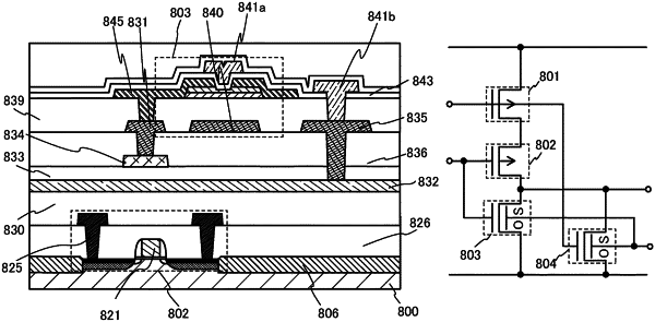
1. A semiconductor device comprising:
a first transistor;
a second transistor;
a third transistor;
a fourth transistor;
a first layer comprising silicon over a substrate;
a first insulating layer over the first layer;
a first gate electrode of the third transistor over the first insulating layer;
a first conductive layer over the first gate electrode of the third transistor, the first conductive layer functioning as a first gate electrode of the second transistor;
a second insulating layer over the first conductive layer;
a second layer comprising an oxide semiconductor over the second insulating layer;
a third insulating layer over the second layer;
a second conductive layer over the third insulating layer, the second conductive layer functioning as a second gate electrode of the second transistor; and
a third conductive layer in contact with a top surface of the second layer,
wherein the second transistor comprises the oxide semiconductor in a channel formation region,
wherein a first wiring is electrically connected to one of a source electrode and a drain electrode of the first transistor,
wherein the other of the source electrode and the drain electrode of the first transistor is electrically connected to one of a source electrode and a drain electrode of the second transistor,
wherein a second wiring is electrically connected to a first gate electrode of the first transistor,
wherein a third wiring is electrically connected to the first gate electrode of the second transistor,
wherein the other of the source electrode and the drain electrode of the second transistor is electrically connected to one of a source electrode and a drain electrode of the third transistor and one of a source electrode and a drain electrode of the fourth transistor,
wherein the first transistor comprises a second gate electrode overlapping with the first gate electrode of the first transistor, and
wherein the third conductive layer comprises a region extending below the second layer.
|