| CPC H01L 29/7786 (2013.01) [H01L 21/7605 (2013.01); H01L 21/765 (2013.01); H01L 29/2003 (2013.01); H01L 29/205 (2013.01); H01L 29/402 (2013.01); H01L 29/66462 (2013.01); H02H 3/06 (2013.01); H02H 3/12 (2013.01)] | 64 Claims |
|
1. An apparatus, comprising:
a substrate;
a group III-Nitride barrier layer;
a source electrically coupled to the group III-Nitride barrier layer;
a gate on the group III-Nitride barrier layer;
a drain electrically coupled to the group III-Nitride barrier layer;
a p-region being arranged at or below the group III-Nitride barrier layer;
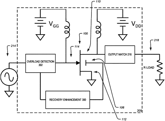
a recovery enhancement circuit configured to reduce an impact of an overload received by the gate; and
a group III-Nitride buffer layer on the substrate,
wherein at least a portion of the p-region is arranged vertically below at least one of the following: the source, the gate, an area between the gate and the drain; and
wherein the group III-Nitride barrier layer is arranged on the group III-Nitride buffer layer, the group III-Nitride barrier layer comprising a higher bandgap than a bandgap of the group III-Nitride buffer layer.
|