| CPC H01L 29/66969 (2013.01) [H01L 21/383 (2013.01); H01L 21/443 (2013.01); H01L 29/401 (2013.01); H01L 27/1207 (2013.01); H01L 29/78648 (2013.01); H01L 29/7869 (2013.01)] | 4 Claims |
|
1. A method for manufacturing a semiconductor device, comprising:
depositing a first oxide semiconductor film;
depositing a first conductive film over the first oxide semiconductor film;
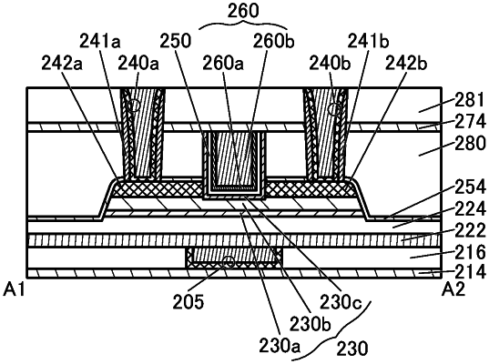
removing part of the first oxide semiconductor film and part of the first conductive film, thereby forming a stacked-layer structure of a first oxide semiconductor and a first conductor;
depositing a first insulating film over the first oxide semiconductor and the first conductor, and then forming a first insulator by planarizing the first insulating film;
forming a second conductor, a third conductor, and an opening exposing part of the first oxide semiconductor by removing part of the first insulator and part of the first conductor;
depositing a second oxide semiconductor film in contact with an exposed region of the first oxide semiconductor;
depositing a second insulating film over the second oxide semiconductor film;
performing microwave-excited plasma treatment on the second insulating film with a pressure of higher than or equal to 400 Pa;
depositing a second conductive film over the second insulating film; and
removing part of the second conductive film, part of the second insulating film, and part of the second oxide semiconductor film, thereby exposing the first insulator and forming a second conductor, a second insulator, and a second oxide semiconductor that are embedded in the opening.
|