| CPC H01L 29/42364 (2013.01) [G02F 1/1368 (2013.01); H01L 27/1225 (2013.01); H01L 29/517 (2013.01); H01L 29/518 (2013.01)] | 16 Claims |
|
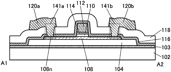
1. A semiconductor device comprising:
a substrate;
a first insulating layer over the substrate;
a second insulating layer over the first insulating layer;
a semiconductor layer over the second insulating layer;
a third insulating layer over the semiconductor layer;
a first gate electrode over the third insulating layer;
a fourth insulating layer over the first gate electrode;
a first conductive layer functioning as one of a source and a drain of a transistor and being electrically connected to the semiconductor layer; and
a second conductive layer functioning as the other of the source and the drain of the transistor and being electrically connected to the semiconductor layer,
wherein, in a cross-sectional view in a channel width direction, an entire top surface of the second insulating layer is covered by a bottom surface of the fourth insulating layer, a bottom surface of the semiconductor layer, and a bottom surface of the third insulating layer.
|