| CPC H01L 29/4236 (2013.01) [H01L 29/401 (2013.01); H01L 29/42368 (2013.01); H01L 29/512 (2013.01); H10B 12/053 (2023.02); H10B 12/34 (2023.02)] | 14 Claims |
|
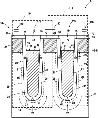
5. A recessed access device comprising:
a conductive gate in a trench in semiconductor material;
a gate insulator extending along sidewalls and around a bottom of the conductive gate between the conductive gate and the semiconductor material;
a pair of source/drain regions in upper portions of the semiconductor material on opposing lateral sides of the trench;
a channel region in the semiconductor material below the pair of source/drain regions extending along sidewalls and around a bottom of the trench;
the gate insulator comprising a low-k material and a high-k material, the low-k material being characterized by its dielectric constant k being no greater than 4.0, the high-k material being characterized by its dielectric constant k being greater than 4.0, the low-k material extending completely along all of the sidewalls of and directly under the bottom of the conductive gate, the high-k material being laterally-inward of the low-k material and at least one of (a) and (b), where:
(a): extending less-than-completely along all of the sidewalls of the conductive gate; and
(b): not being directly under the bottom of the conductive gate;
comprising the (a); and
comprising the (a) and the (b).
|