| CPC H01L 29/41758 (2013.01) [H01L 29/2003 (2013.01); H01L 29/402 (2013.01); H01L 29/42316 (2013.01); H01L 29/7786 (2013.01)] | 20 Claims |
|
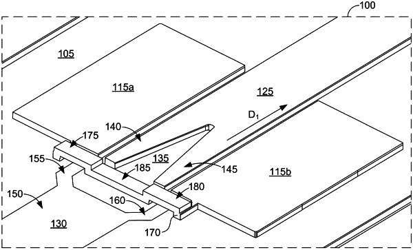
1. A field effect transistor, comprising:
a first source metal;
a second source metal;
a gate manifold comprising a gate manifold body, a first angled gate tab, and a second angled gate tab; and
a drain metal positioned between the first source metal and the second source metal over a channel of the field effect transistor, wherein the drain metal comprises a drain metal body having a notched region between the first source metal and the second source metal over the channel, the notched region defining a first projecting portion and a second projecting portion of the drain metal body, the first projecting portion and the second projecting portion positioned on respective sides of the notched region.
|