| CPC H01L 29/401 (2013.01) [H01L 29/407 (2013.01); H01L 29/512 (2013.01); H01L 29/513 (2013.01); H01L 29/66734 (2013.01); H01L 29/7813 (2013.01); H01L 21/28194 (2013.01); H01L 21/28202 (2013.01); H01L 21/28229 (2013.01); H01L 29/518 (2013.01)] | 9 Claims |
|
1. A method of manufacturing a semiconductor device, comprising:
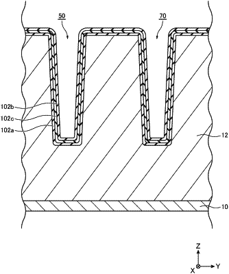
forming a trench in a semiconductor layer of first conductivity type;
in the trench, forming a first layer containing silicon on an inner surface of the trench and then forming a second layer containing first oxide or nitride on the first layer, or forming the second layer on the inner surface of the trench and then forming the first layer on the second layer; and
thermally oxidizing the first layer.
|