| CPC H01L 28/40 (2013.01) [H10B 12/315 (2023.02)] | 13 Claims |
|
1. A method of manufacturing an integrated circuit device comprising:
forming a lower electrode on a substrate;
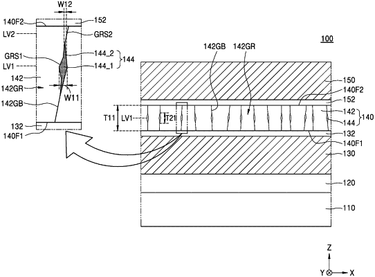
forming a first dielectric layer on the lower electrode, the first dielectric layer including at least two grains and a grain boundary region that is disposed between the at least two grains, the first dielectric layer including a lower portion, an upper portion, and a middle portion that is disposed between the lower portion and the upper portion;
forming a second dielectric layer in the first dielectric layer;
forming an upper electrode on the first dielectric layer;
forming a first interface layer that is disposed between the lower electrode and the first dielectric layer; and
forming a second interface layer that is disposed between the first dielectric layer and the upper electrode,
wherein the second dielectric layer is formed in the grain boundary region of the middle portion of the first dielectric layer such that a width of the second dielectric layer in the middle portion is greater than a width of the second dielectric layer in at least one of the upper or lower portions when viewed in cross section,
the lower electrode includes titanium nitride,
the first interface layer includes titanium oxide and niobium oxide,
the first dielectric layer includes hafnium oxide and zirconium oxide,
the second dielectric layer includes aluminium oxide,
the second interface layer includes titanium oxide, and
the upper electrode includes titanium nitride.
|