| CPC H01L 27/14647 (2013.01) [H01L 31/035209 (2013.01)] | 20 Claims |
|
1. An image sensor, comprising:
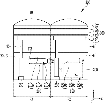
a first photo-sensing device on a semiconductor substrate, the first photo-sensing device being configured to sense light in a first wavelength spectrum associated with a first color;
a second photo-sensing device integrated in the semiconductor substrate, the second photo-sensing device being configured to sense light in a second wavelength spectrum associated with a second color; and
a third photo-sensing device integrated in the semiconductor substrate, the third photo-sensing device being configured to sense light in a third wavelength spectrum associated with a third color,
wherein the first photo-sensing device and the second photo-sensing device are overlapped with each other in a thickness direction of the semiconductor substrate, the thickness direction being perpendicular to an upper surface of the semiconductor substrate,
wherein the first photo-sensing device and the third photo-sensing device are overlapped with each other in the thickness direction of the semiconductor substrate,
wherein the second photo-sensing device and the third photo-sensing device each include
an upper surface that is proximate to the upper surface of the semiconductor substrate,
a lower surface facing the upper surface and distal from the upper surface of the semiconductor substrate, and
a doped region between the upper surface and the lower surface,
wherein the upper surface of the third photo-sensing device is distal from the upper surface of the semiconductor substrate in relation to the upper surface of the second photo-sensing device,
wherein a wavelength selectivity of the third wavelength spectrum relative to the second wavelength spectrum of the third photo-sensing device varies depending on a depth of the upper surface of the third photo-sensing device from the upper surface of the semiconductor substrate in the thickness direction, and
wherein the depth of the upper surface of the third photo-sensing device from the upper surface of the semiconductor substrate in the thickness direction is a depth D3 that satisfies Relationship Equation 1,
EQE(λ3)≥3×EQE(λ2) [Relationship Equation 1]
wherein, in Relationship Equation 1,
EQE (λ3) is external quantum efficiency at a wavelength (λ3) included in the third wavelength spectrum of the third photo-sensing device based on the depth of the upper surface of the third photo-sensing device in the semiconductor substrate being the depth D3, and
EQE (λ2) is external quantum efficiency at a wavelength (λ2) included in the second wavelength spectrum of the third photo-sensing device based on the depth of the upper surface of the third photo-sensing device in the semiconductor substrate being the depth D3.
|