| CPC H01L 27/14643 (2013.01) [H01L 27/14612 (2013.01); H01L 27/14621 (2013.01); H01L 27/14636 (2013.01); H01L 27/14689 (2013.01); H04N 25/60 (2023.01)] | 20 Claims |
|
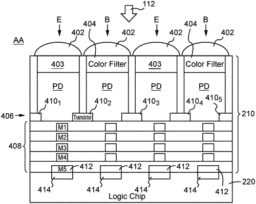
1. An apparatus, comprising a first electronic chip having an array of photosensitive pixels along a light-receiving surface thereof, wherein a pixel of the array comprises:
one or more first photodiodes and one or more second photodiodes;
first and second transistors; and
an interconnect structure vertically below the first and second photodiodes and the first and second transistors, the interconnect structure including first electrical conductors interconnecting the one or more first photodiodes and the first transistors to form a first electrical circuit and further including second electrical conductors interconnecting the one or more second photodiodes and the second transistors to form a second electrical circuit, the first and second electrical circuits being functionally different and independent from each other;
wherein the first electrical conductors are arranged substantially in a portion of the interconnect structure vertically below a first area of the light-receiving surface in the pixel; and
wherein the second electrical conductors are arranged substantially in a portion of the interconnect structure vertically below a second area of the light-receiving surface in the pixel, the second area non-overlapping with the first area.
|