| CPC H01L 27/14643 (2013.01) [B23K 26/355 (2018.08); B82Y 40/00 (2013.01); H01L 27/14625 (2013.01); H01L 27/14629 (2013.01); H01L 27/1463 (2013.01); H01L 27/14632 (2013.01); H01L 27/1464 (2013.01); H01L 27/14689 (2013.01); H01L 31/02327 (2013.01); H01L 31/028 (2013.01); H01L 31/182 (2013.01)] | 20 Claims |
|
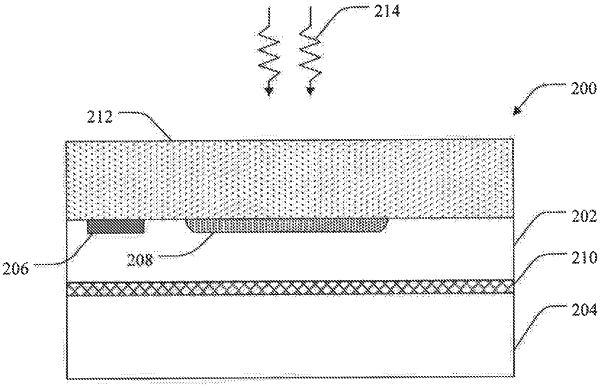
1. An optoelectronic image sensor device having enhanced absorption of electromagnetic radiation, comprising:
a semiconductor layer coupled to a support substrate; and
an array of shallow trench isolation surface features formed on at least a portion of a surface of the support substrate and positioned between the semiconductor layer and the support substrate, the surface features positioned to interact with electromagnetic radiation that passes through the semiconductor layer.
|