US 11,929,380 B2
Solid-state image-capturing element having floation diffusion and hollow regions
Yusuke Tanaka, Kanagawa (JP); Takashi Nagano, Kanagawa (JP); Toshifumi Wakano, Kanagawa (JP); and Takeshi Matsunuma, Kanagawa (JP)
Assigned to SONY SEMICONDUCTOR SOLUTIONS CORPORATION, Kanagawa (JP)
Filed by SONY SEMICONDUCTOR SOLUTIONS CORPORATION, Kanagawa (JP)
Filed on Oct. 14, 2021, as Appl. No. 17/501,135.
Application 17/501,135 is a continuation of application No. 17/015,291, filed on Sep. 9, 2020, granted, now 11,183,528.
Application 17/015,291 is a continuation of application No. 16/507,663, filed on Jul. 10, 2019, granted, now 10,797,097, issued on Oct. 6, 2020.
Application 16/507,663 is a continuation of application No. 15/556,902, granted, now 10,396,116, issued on Aug. 27, 2019, previously published as PCT/JP2016/058453, filed on Mar. 17, 2016.
Claims priority of application No. 2015-071024 (JP), filed on Mar. 31, 2015; and application No. 2015-200339 (JP), filed on Oct. 8, 2015.
Prior Publication US 2022/0037389 A1, Feb. 3, 2022
Int. Cl. H01L 27/14 (2006.01); H01L 27/146 (2006.01); H01L 29/78 (2006.01); H04N 25/62 (2023.01); H04N 25/70 (2023.01); H04N 25/79 (2023.01); H01L 29/06 (2006.01); H01L 29/49 (2006.01); H01L 29/51 (2006.01); H04N 25/75 (2023.01); H04N 25/76 (2023.01); H10B 12/00 (2023.01)
CPC H01L 27/14636 (2013.01) [H01L 27/14603 (2013.01); H01L 27/14612 (2013.01); H01L 27/14634 (2013.01); H01L 27/14641 (2013.01); H01L 27/14683 (2013.01); H01L 27/1469 (2013.01); H04N 25/62 (2023.01); H04N 25/70 (2023.01); H04N 25/79 (2023.01); H01L 27/14643 (2013.01); H01L 27/14649 (2013.01); H01L 27/14689 (2013.01); H01L 29/0649 (2013.01); H01L 29/4991 (2013.01); H01L 29/515 (2013.01); H01L 29/7841 (2013.01); H04N 25/75 (2023.01); H04N 25/76 (2023.01); H10B 12/20 (2023.02)] 12 Claims
OG exemplary drawing
 
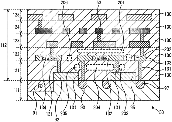
1. A semiconductor device, comprising:
a semiconductor substrate including an impurity region; and
a wiring layer including:
a first via connected to the impurity region;
a second via;
a first hollow region, wherein
the first hollow region is between the first via and the second via, and
the first via is not in contact with the first hollow region; and
a second hollow region, wherein the second via is between the first via and the second hollow region.