US 11,929,376 B2
Solid-state imaging device and imaging apparatus
Tetsuji Yamaguchi, Kanagawa (JP)
Assigned to Sony Group Corporation, Tokyo (JP)
Filed by Sony Group Corporation, Tokyo (JP)
Filed on Mar. 15, 2023, as Appl. No. 18/184,295.
Application 18/184,295 is a continuation of application No. 18/078,734, filed on Dec. 9, 2022.
Application 18/078,734 is a continuation of application No. 17/400,270, filed on Aug. 12, 2021, granted, now 11,569,281, issued on Jan. 31, 2023.
Application 17/400,270 is a continuation of application No. 16/892,925, filed on Jun. 4, 2020, granted, now 11,227,884, issued on Jan. 18, 2022.
Application 16/892,925 is a continuation of application No. 16/359,209, filed on Mar. 20, 2019, granted, now 10,715,768, issued on Jul. 14, 2020.
Application 16/359,209 is a continuation of application No. 15/674,890, filed on Aug. 11, 2017, granted, now 10,271,023, issued on Apr. 23, 2019.
Application 15/674,890 is a continuation of application No. 15/273,289, filed on Sep. 22, 2016, granted, now 9,762,867, issued on Sep. 12, 2017.
Application 15/273,289 is a continuation of application No. 15/086,890, filed on Mar. 31, 2016, granted, now 9,466,645, issued on Oct. 11, 2016.
Application 15/086,890 is a continuation of application No. 14/613,002, filed on Feb. 3, 2015, granted, now 9,369,647, issued on Jun. 14, 2016.
Application 14/613,002 is a continuation of application No. 14/348,992, granted, now 9,018,688, issued on Apr. 28, 2015, previously published as PCT/JP2012/075041, filed on Sep. 28, 2012.
Claims priority of application No. 2011-223856 (JP), filed on Oct. 11, 2011.
Prior Publication US 2023/0282658 A1, Sep. 7, 2023
Int. Cl. H01L 27/146 (2006.01); H01L 31/101 (2006.01); H04N 9/64 (2023.01); H04N 23/75 (2023.01); H04N 23/88 (2023.01); H04N 25/11 (2023.01); H04N 25/70 (2023.01); H04N 25/71 (2023.01); H04N 25/711 (2023.01); H04N 25/75 (2023.01); H10K 39/32 (2023.01)
CPC H01L 27/14614 (2013.01) [H01L 27/14638 (2013.01); H01L 27/1464 (2013.01); H01L 27/14645 (2013.01); H01L 27/14647 (2013.01); H01L 31/1013 (2013.01); H04N 9/646 (2013.01); H04N 23/75 (2023.01); H04N 23/88 (2023.01); H04N 25/11 (2023.01); H04N 25/70 (2023.01); H04N 25/71 (2023.01); H04N 25/711 (2023.01); H04N 25/75 (2023.01); H10K 39/32 (2023.02)] 12 Claims
OG exemplary drawing
 
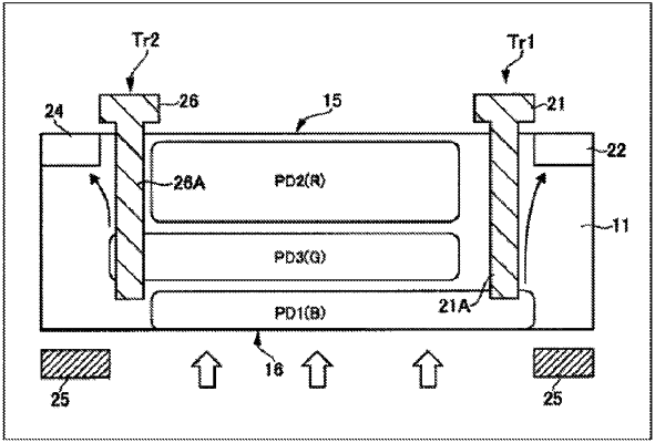
1. A light detecting device, comprising:
a first photoelectric conversion unit disposed above a substrate, the substrate comprising a first surface and a second surface opposite to the first surface, the first surface being disposed between the first photoelectric conversion unit and the second surface, and the first photoelectric conversion unit comprising:
a first electrode;
a second electrode disposed between the first electrode and the substrate; and
a photoelectric conversion layer disposed between the first electrode and the second electrode;
a second photoelectric conversion unit disposed in the substrate, the second photoelectric conversion unit overlapping the first photoelectric conversion unit in a plan view;
a gate electrode, at least a portion of the gate electrode being disposed in the substrate and overlapping the second photoelectric conversion unit in the plan view;
a wiring layer disposed between the first surface of the substrate and the second electrode; and
a first floating diffusion region disposed in the substrate, the first floating diffusion region being disposed at a side of the second surface,
wherein at least a portion of the second photoelectric conversion unit is disposed between the first surface and the gate electrode, and
wherein the first floating diffusion region is configured to receive a charge generated in the photoelectric conversion layer through at least the second electrode and the wiring layer.