| CPC H01L 27/14612 (2013.01) [H01L 27/14605 (2013.01); H04N 25/77 (2023.01)] | 20 Claims |
|
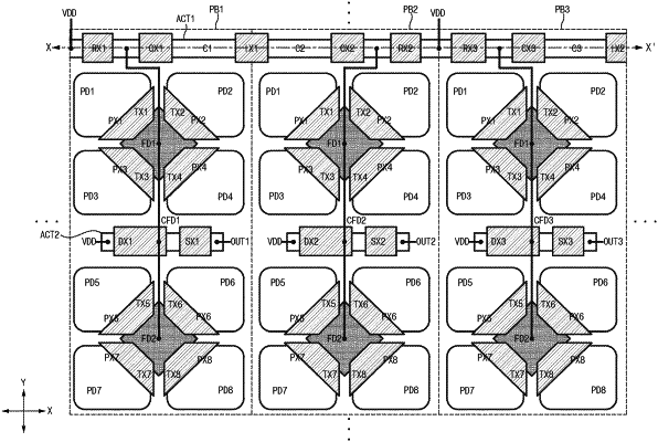
1. An image sensing device, comprising:
a first unit pixel block that includes a first common floating diffusion node, a plurality of first photoelectric conversion elements configured to generate photocharges through conversion of incident light, a plurality of first transfer transistors configured to transmit the photocharges generated by the plurality of first photoelectric conversion elements to the first common floating diffusion node, and a first conversion gain transistor configured to change capacitance of the first common floating diffusion node;
a second unit pixel block adjacent to the first unit pixel block in a first direction, that includes a second common floating diffusion node, a plurality of second photoelectric conversion elements configured to generate photocharges through conversion of incident light, a plurality of second transfer transistors configured to transmit the photocharges generated by the plurality of second photoelectric conversion elements to the second common floating diffusion node, and a second conversion gain transistor configured to change capacitance of the second common floating diffusion node; and
an isolation transistor located in a boundary region between the first unit pixel block and the second unit pixel block, and configured to isolate the first conversion gain transistor and the second conversion gain transistor from each other.
|