| CPC H01L 27/0886 (2013.01) [H01L 21/3086 (2013.01); H01L 21/823431 (2013.01); H01L 21/823437 (2013.01); H01L 21/823468 (2013.01); H01L 21/823481 (2013.01); H01L 29/66545 (2013.01); H01L 29/66553 (2013.01); H01L 29/6656 (2013.01); H01L 29/66795 (2013.01); H01L 29/7851 (2013.01)] | 20 Claims |
|
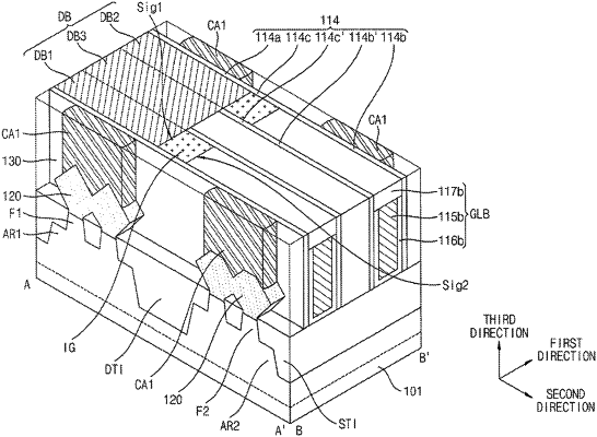
1. A semiconductor device, comprising:
a substrate having a first region and a second region;
first active fins that extend in a first direction in the first region;
second active fins that extend in the first direction in the second region;
a first field insulating layer between the first active fins and extending in a second direction;
a second field insulating layer between the second active fins and extending in the second direction;
a gate line that extends in the second direction on the second field insulating layer and on a straight line with the first field insulating layer along the second direction; and
a gate isolation layer between the first field insulating layer and the gate line,
wherein:
the gate line includes a gate electrode, a gate insulating layer on a lower surface and a side surface of the gate electrode, and a gate capping layer on an upper surface of the gate electrode,
a first side surface of the gate isolation layer in the second direction is in contact with a portion of the gate insulating layer, and
an upper surface of the gate isolation layer is at substantially a same level as an upper surface of the gate capping layer.
|