| CPC H01L 27/0605 (2013.01) [H01L 21/0254 (2013.01); H01L 21/743 (2013.01); H01L 21/746 (2013.01); H01L 21/7605 (2013.01); H01L 21/76202 (2013.01); H01L 21/8252 (2013.01); H01L 23/5286 (2013.01); H01L 23/535 (2013.01); H01L 23/66 (2013.01); H01L 29/0649 (2013.01); H01L 29/2003 (2013.01)] | 20 Claims |
|
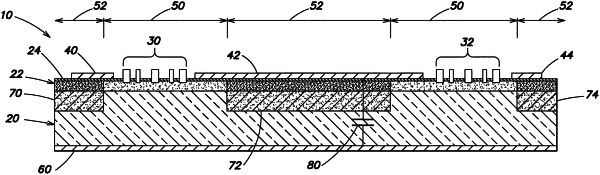
1. A semiconductor structure, comprising:
a substrate;
a low dielectric constant material region in the substrate, the low dielectric constant material region comprising an oxide and being positioned between a first device area in the semiconductor structure and a second device area in the semiconductor structure, a dielectric constant of the low dielectric constant material region being lower than a dielectric constant of the substrate;
a III-nitride material layer over the substrate, the III-nitride material layer extending over the substrate in the first device area, over the low dielectric constant material region, and over the substrate in the second device area;
a first device formed in the III-nitride material layer in the first device area;
a second device in the III-nitride material layer in the second device area; and
an interconnect formed over the low dielectric constant material region, the interconnect comprising a metal interconnect line that provides a continuous conductive path of metal from the first device area, over the low dielectric constant material region, and to the second device area.
|