| CPC H01L 27/0259 (2013.01) [H01L 29/0821 (2013.01); H01L 29/6625 (2013.01); H01L 29/735 (2013.01)] | 14 Claims |
|
1. A method of manufacturing a semiconductor integrated circuit device, the method comprising:
providing a semiconductor substrate having a first conductivity type;
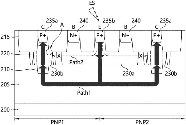
forming a body contact region in the semiconductor substrate, the body contact region including first impurities having the first conductivity type;
forming isolation layers in the semiconductor substrate;
implanting second impurities with a second conductivity type opposite to the first conductivity type to the semiconductor substrate, thereby forming a first well which is spaced from the body contact region and a second well which contacts with a sidewall of the body contact region; and
forming a base and an emitter in the first well between the isolation layers and forming a collector in the body contact region,
wherein the first well and the second well are formed to have a same depth.
|