| CPC H01L 25/0657 (2013.01) [H01L 24/08 (2013.01); H01L 25/18 (2013.01); H01L 2224/08145 (2013.01); H01L 2225/06524 (2013.01); H01L 2924/1431 (2013.01); H01L 2924/14511 (2013.01)] | 18 Claims |
|
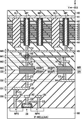
1. A memory chip comprising:
a set of first word lines, which are stacked along a first direction and extend in a first region and a second region of the memory chip along a second direction crossing the first direction;
a pillar including:
a semiconductor layer extending through the first word lines along the first direction in the first region, and
an insulating layer between the semiconductor layer and the first word lines;
a set of memory cells in the first region, each of which is disposed at a corresponding intersection of the pillar and one of the first word lines;
a set of bonding pads in the second region; and
a set of transistors in the second region, each of which is configured to electrically connect or disconnect a corresponding one of the first word lines to or from a corresponding one of the bonding pads, wherein
a number of bonding pads in the set of bonding pads is smaller than a number of transistors in the set of transistors.
|