| CPC H01L 24/08 (2013.01) [H01L 23/5228 (2013.01); H01L 25/0657 (2013.01); H01L 25/18 (2013.01); H01L 2224/08145 (2013.01); H01L 2924/1431 (2013.01); H01L 2924/14511 (2013.01); H01L 2924/19043 (2013.01); H01L 2924/19104 (2013.01)] | 9 Claims |
|
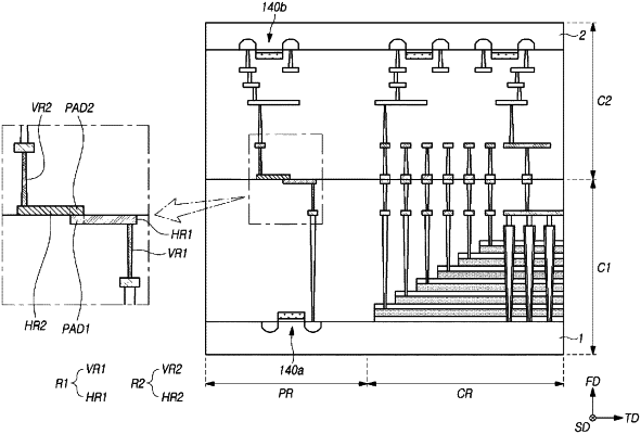
1. A semiconductor device comprising:
a first pad defined on one surface of a first chip, the first chip includes a memory cell array disposed in a cell region and a first peripheral circuit disposed in a peripheral region outside of the cell region;
a second pad defined on one surface of a second chip, which is stacked on the first chip in a first direction, and bonded to the first pad, the second chip includes a second peripheral circuit disposed in the peripheral region;
a first horizontal resistor pattern defined on the one surface of the first chip and coupled to the first pad; and
a second horizontal resistor pattern defined on the one surface of the second chip and coupled to the second pad,
wherein the first horizontal resistor pattern and the second horizontal resistor pattern are disposed between the first peripheral circuit and the second peripheral circuit in the peripheral region,
wherein the first horizontal resistor pattern and the second horizontal resistor pattern do not overlap with each other in the first direction.
|