| CPC H01L 23/528 (2013.01) [G11C 5/10 (2013.01); H01L 21/76831 (2013.01); H01L 29/0649 (2013.01); H01L 29/4236 (2013.01); H10B 12/485 (2023.02)] | 20 Claims |
|
1. A semiconductor device, comprising:
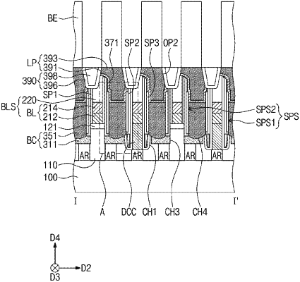
a substrate including a first device isolation region, a second device isolation region having a first side and a second side opposite the first side, a first active region between the first device isolation region and the first side of the second device isolation region, and a second active region adjacent to the second side of the second device isolation region;
a first bit line structure on the first device isolation region;
a second bit line structure on the second active region;
a buffer pattern between the first device isolation region and the first bit line structure;
a first contact between the first bit line structure and the second bit line structure, the first contact including a first portion, a second portion that is on the first portion, and a third portion that is on the second portion;
a second contact between the second active region and the second bit line structure;
a first spacer structure between the first bit line structure and the first contact, the first spacer structure including a first sub-spacer, a second sub-spacer that is on the first sub-spacer, and a third sub-spacer that is on the second sub-spacer; and
a capacitor bottom electrode on the first contact,
wherein the first portion of the first contact is in contact with the first device isolation region, the first active region and the second device isolation region,
wherein the first sub-spacer of the first spacer structure is in contact with a top surface of the buffer pattern,
wherein the second sub-spacer of the first spacer structure is in contact with the buffer pattern, the first device isolation region and the first portion of the first contact, and
wherein a top surface of the first portion of the first contact is lower than a top surface of the first device isolation region.
|