| CPC H01L 23/5226 (2013.01) [H01L 24/19 (2013.01); H01L 24/20 (2013.01); H01L 25/105 (2013.01); H01L 25/50 (2013.01); H01L 21/311 (2013.01); H01L 21/568 (2013.01); H01L 23/3128 (2013.01); H01L 25/0657 (2013.01); H01L 2224/04105 (2013.01); H01L 2224/12105 (2013.01); H01L 2224/32145 (2013.01); H01L 2224/32225 (2013.01); H01L 2224/48091 (2013.01); H01L 2224/48227 (2013.01); H01L 2224/73265 (2013.01); H01L 2224/73267 (2013.01); H01L 2224/92244 (2013.01); H01L 2225/0651 (2013.01); H01L 2225/06568 (2013.01); H01L 2225/1035 (2013.01); H01L 2225/1041 (2013.01); H01L 2225/1058 (2013.01); H01L 2924/15311 (2013.01); H01L 2924/181 (2013.01)] | 20 Claims |
|
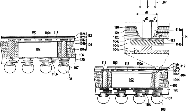
1. A manufacturing method of a package structure, comprising:
forming a dielectric layer over a carrier;
providing a die and forming a conductive structure on the dielectric layer and beside the die;
forming an encapsulant surrounding the die and covering the conductive structure;
debonding the carrier and exposing the dielectric layer overlying the conductive structure;
laser drilling an opening in the dielectric layer to expose a first area of a top surface of the conductive structure; and
widening the opening by an etching process to expose a second area of the top surface of the conductive structure, wherein the first area is smaller than the second area.
|