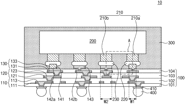
| CPC H01L 23/49838 (2013.01) [H01L 21/481 (2013.01); H01L 21/4857 (2013.01); H01L 23/49822 (2013.01); H01L 24/13 (2013.01); H01L 24/16 (2013.01); H01L 24/17 (2013.01); H01L 24/81 (2013.01); H01L 21/561 (2013.01); H01L 21/563 (2013.01); H01L 23/3107 (2013.01); H01L 24/73 (2013.01); H01L 25/18 (2013.01); H01L 2224/13016 (2013.01); H01L 2224/13541 (2013.01); H01L 2224/1355 (2013.01); H01L 2224/16013 (2013.01); H01L 2224/1607 (2013.01); H01L 2224/16227 (2013.01); H01L 2224/16238 (2013.01); H01L 2224/17055 (2013.01); H01L 2224/17517 (2013.01); H01L 2224/73204 (2013.01); H01L 2224/81345 (2013.01); H01L 2224/81815 (2013.01)] | 20 Claims |

|
1. A method of fabricating a semiconductor package, the method comprising:
forming a redistribution substrate that includes a dielectric pattern and a redistribution pattern buried in the dielectric pattern;
forming a seed layer on the redistribution substrate;
forming a mask pattern on the seed layer, the mask pattern having a first opening with a first width and a second opening with a second width less than the first width;
performing a plating process in which the seed layer is used as a seed to form a first substrate pad that fills the first opening and a second substrate pad that fills the second opening;
removing the mask pattern and an exposed portion of the seed layer;
providing a plurality of connection members on corresponding chip pads of a semiconductor chip;
placing the semiconductor chip on the redistribution substrate to allow the connection members to rest on the first substrate pad and the second substrate pad; and
performing on the connection members a reflow process to form a first connection terminal that connects the first substrate pad to a first chip pad of the chip pads of the semiconductor chip and a second connection terminal that connects the second substrate pad to a second chip pad of the chip pads of the semiconductor chip,
wherein each of the first and second chip pads has a quadrilateral shape when viewed in cross-section,
wherein a maximum width of the first substrate pad is substantially the same as widths of the first and second chip pads, and
wherein a maximum width of the second substrate pad is less than the widths of the first and second chip pads.
|