| CPC H01L 23/49816 (2013.01) [H01L 23/15 (2013.01); H01L 23/32 (2013.01); H01L 23/49838 (2013.01); H01L 24/16 (2013.01); H01L 24/73 (2013.01); H01L 24/81 (2013.01); H01L 31/02002 (2013.01); H04N 23/54 (2023.01); H01L 2224/16225 (2013.01); H01L 2224/32225 (2013.01); H01L 2224/73204 (2013.01)] | 19 Claims |
|
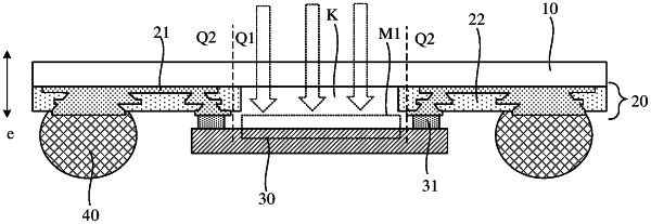
1. A chip package structure, comprising:
a substrate comprising a first region and a second region surrounding the first region;
a wiring layer located on a side of the substrate and comprising at least one metal wire, wherein at least part of a metal wire of the at least one metal wire is in contact with the substrate, and wherein the at least one metal wire overlaps with the second region in a direction perpendicular to the substrate;
a chip located on a side of the wiring layer facing away from the substrate, wherein the chip corresponds to the first region, wherein the chip comprises a first conductive bump disposed on a side of the chip facing towards to the substrate, and wherein the first conductive bump is electrically connected to one of the at least one metal wire; and
a second conductive bump electrically connected to one of the at least one metal wire, wherein the second conductive bump does not overlap with the chip in the direction perpendicular to the substrate;
wherein the chip comprises a photosensitive region located at the side of the chip facing towards the substrate and opposite to the first region, and wherein the photosensitive region does not overlap with the metal wire in the wiring layer.
|