| CPC H01L 23/4825 (2013.01) [H01L 21/822 (2013.01); H01L 27/0292 (2013.01); H01L 21/56 (2013.01); H01L 27/0255 (2013.01)] | 11 Claims |
|
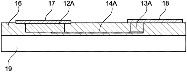
1. A method, comprising:
forming a first electrostatic discharge protection device structure in a first area on a front side of a semiconductor substrate;
forming a first contact pad on the first electrostatic discharge protection device structure and a second contact pad in a second area on the front side of the semiconductor substrate;
thinning the semiconductor substrate from a back side of the semiconductor substrate;
forming a metal connection connecting the first electrostatic discharge protection device structure to the second area; and
providing a carrier material to the back side of the semiconductor substrate after forming the metal connection.
|