| CPC H01L 23/3171 (2013.01) [H01L 21/02164 (2013.01); H01L 21/02274 (2013.01); H01L 21/31053 (2013.01); H01L 21/7685 (2013.01); H01L 23/291 (2013.01)] | 11 Claims |
|
1. A method of forming a semiconductor device, said method comprising the steps of:
providing a metal component having a top surface, a first side and an opposite second side;
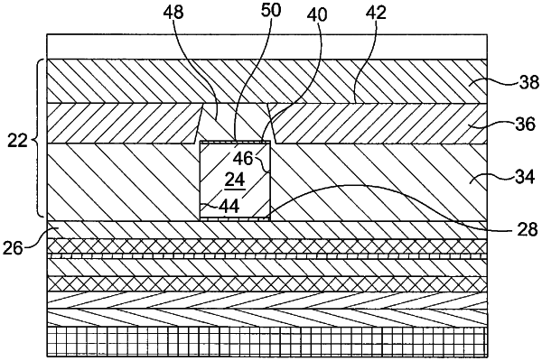
providing a passivation layer over said metal component such that an outer layer of said passivation layer is substantially planar and does not extend below said top surface of said metal component, wherein said step of providing a passivation layer comprises:
depositing over said metal component a substantially planar High Density Plasma Silicon Dioxide (HDP SiO2) layer;
depositing over said HDP SiO2 layer a substantially planar Silicon Rich Oxide (SRO) layer; and
performing Chemical Mechanical Planarization (CMP) of said HDP SiO2 and SRO layers to form a planar surface, wherein said HDP SiO2 layer is substantially planar in regions on said first and second sides of said metal component, and has a top surface which is at a same height as said top surface of said metal component in said regions.
|