| CPC H01L 21/823821 (2013.01) [H01L 21/28088 (2013.01); H01L 21/823814 (2013.01); H01L 21/823842 (2013.01); H01L 21/845 (2013.01); H01L 27/088 (2013.01); H01L 27/092 (2013.01); H01L 27/0924 (2013.01); H01L 27/1211 (2013.01); H01L 29/4966 (2013.01); H01L 29/513 (2013.01); H01L 29/517 (2013.01); H01L 29/66545 (2013.01)] | 20 Claims |
|
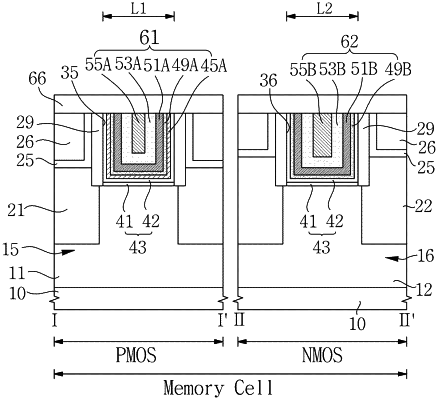
1. A semiconductor device comprising:
a substrate;
a first fin active area and a second fin active area on the substrate;
a first gate dielectric layer on the first fin active area;
a first gate electrode on the first gate dielectric layer, the first gate electrode including
a first layer on the first gate dielectric and including TiN,
a second layer on the first layer and including TiAlC and TiN,
a third layer on the second layer and including TiN, and
a fourth layer on the third layer and including W;
a first spacer on a sidewall of the first gate dielectric layer and the first gate electrode;
a second gate dielectric layer on the second fin active area;
a second gate electrode on the second gate dielectric layer, the second gate electrode including
a fifth layer on the second gate dielectric layer and including TiAlC and TiN,
a sixth layer on the fifth layer and including TiN, and
a seventh layer on the sixth layer and including W;
a second spacer on a sidewall of the second gate dielectric layer and the second gate electrode; and
wherein a second width of the seventh layer is greater than a first width of the fourth layer,
wherein upper surfaces of the first gate dielectric layer, the first gate electrode, and the first spacer are coplanar, and
wherein upper surfaces of the second gate dielectric layer, the second gate electrode, and the second spacer are coplanar.
|