US 11,929,285 B2
Backside metal patterning die singulation system and related methods
Michael J. Seddon, Gilbert, AZ (US)
Assigned to SEMICONDUCTOR COMPONENTS INDUSTRIES, LLC, Scottsdale, AZ (US)
Filed by SEMICONDUCTOR COMPONENTS INDUSTRIES, LLC, Phoenix, AZ (US)
Filed on Jan. 11, 2023, as Appl. No. 18/153,133.
Application 18/153,133 is a continuation of application No. 17/216,167, filed on Mar. 29, 2021, granted, now 11,581,223.
Application 17/216,167 is a continuation of application No. 16/505,878, filed on Jul. 9, 2019, granted, now 10,964,596, issued on Mar. 30, 2021.
Claims priority of provisional application 62/796,659, filed on Jan. 25, 2019.
Prior Publication US 2023/0170259 A1, Jun. 1, 2023
This patent is subject to a terminal disclaimer.
Int. Cl. H01L 21/78 (2006.01); H01L 21/027 (2006.01); H01L 21/268 (2006.01); H01L 21/32 (2006.01); H01L 21/3205 (2006.01); H01L 21/3213 (2006.01); H01L 21/66 (2006.01); H01L 23/544 (2006.01)
CPC H01L 21/78 (2013.01) [H01L 21/0274 (2013.01); H01L 21/268 (2013.01); H01L 21/32 (2013.01); H01L 21/32051 (2013.01); H01L 21/32131 (2013.01); H01L 22/20 (2013.01); H01L 23/544 (2013.01); H01L 2223/5446 (2013.01)] 20 Claims
OG exemplary drawing
 
1. A method of aligning a substrate, the method comprising:
forming a plurality of die on a first side of the substrate;
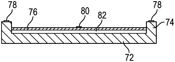
thinning a second side of the substrate and forming an edge ring through the thinning;
forming a backside metal layer on the second side of the substrate;
applying a photoresist layer over the backside metal layer; and
aligning the substrate from the second side of the substrate using a plurality of alignment features comprised one of in the edge ring or on the photoresist layer.