| CPC H01L 21/67103 (2013.01) [H01J 37/05 (2013.01); H01J 37/20 (2013.01); H01J 37/3171 (2013.01); H01L 21/6833 (2013.01); H01J 2237/2007 (2013.01); H01J 2237/20235 (2013.01)] | 20 Claims |
|
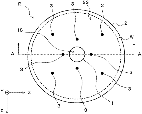
1. A wafer supporting device comprising:
a support base having a wafer-facing surface, the support base comprising a heater; and
an electrostatic chuck supported by the support base, the electrostatic chuck having an attraction surface configured to attract a wafer for wafer processing,
wherein, during the wafer processing, the wafer-facing surface and the attraction surface are positioned at respective different positions in a direction perpendicular to the wafer-facing surface so that the attraction surface is separated from the wafer-facing surface by a distance, and
wherein a size of the wafer is greater than a size of the attraction surface and an area of the wafer that is not supported by the attraction surface of the electrostatic chuck is larger than an area of the wafer that is supported by the attraction surface of the electrostatic chuck.
|