| CPC H01L 21/563 (2013.01) [H01L 21/565 (2013.01); H01L 23/49816 (2013.01); H01L 24/45 (2013.01); H01L 25/0657 (2013.01); H01L 25/105 (2013.01); H01L 25/50 (2013.01); H01L 23/49811 (2013.01); H01L 24/13 (2013.01); H01L 24/16 (2013.01); H01L 24/32 (2013.01); H01L 24/48 (2013.01); H01L 24/73 (2013.01); H01L 24/92 (2013.01); H01L 25/0655 (2013.01); H01L 2224/131 (2013.01); H01L 2224/13111 (2013.01); H01L 2224/16225 (2013.01); H01L 2224/16227 (2013.01); H01L 2224/32225 (2013.01); H01L 2224/45139 (2013.01); H01L 2224/45144 (2013.01); H01L 2224/45147 (2013.01); H01L 2224/45664 (2013.01); H01L 2224/45666 (2013.01); H01L 2224/45669 (2013.01); H01L 2224/45671 (2013.01); H01L 2224/45678 (2013.01); H01L 2224/4568 (2013.01); H01L 2224/45684 (2013.01); H01L 2224/48091 (2013.01); H01L 2224/48227 (2013.01); H01L 2224/73204 (2013.01); H01L 2224/92125 (2013.01); H01L 2225/06517 (2013.01); H01L 2225/0652 (2013.01); H01L 2225/1023 (2013.01); H01L 2225/1058 (2013.01); H01L 2924/1432 (2013.01); H01L 2924/1434 (2013.01); H01L 2924/1436 (2013.01); H01L 2924/1437 (2013.01); H01L 2924/1438 (2013.01); H01L 2924/15311 (2013.01); H01L 2924/15321 (2013.01); H01L 2924/1533 (2013.01)] | 20 Claims |
|
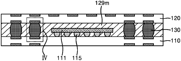
1. A stack package, comprising:
a first package substrate including a first surface on which a first semiconductor device is mounted;
a second package substrate provided on the first semiconductor device, the second package substrate including a first surface facing the first surface of the first package substrate;
a connection terminal connecting the first semiconductor device and the first package substrate;
a connector connecting a terminal on the first surface of the first package substrate and a terminal on the first surface of the second package substrate corresponding thereto; and
molding resin encircling the connector while filling a portion between the first package substrate and the second package substrate,
wherein a portion of the molding resin encircles the connection terminal while, without using an underfill, filling a portion between the first semiconductor device and the first package substrate and completely filling a space between an upper surface of the first semiconductor device and a lower surface of the second package substrate, and
wherein the connector having a largest horizontal cross-sectional area at a center portion and the farther the horizontal cross-sectional area is from the center portion, the horizontal cross-sectional area decreases gradually.
|