| CPC H01L 21/4821 (2013.01) [H01L 23/3121 (2013.01); H01L 23/49503 (2013.01); H01L 23/49513 (2013.01); H01L 23/49541 (2013.01); H01L 23/49575 (2013.01); H01L 24/45 (2013.01); H01L 24/48 (2013.01); H01L 21/561 (2013.01); H01L 21/565 (2013.01); H01L 24/32 (2013.01); H01L 24/73 (2013.01); H01L 24/83 (2013.01); H01L 24/85 (2013.01); H01L 24/92 (2013.01); H01L 24/97 (2013.01); H01L 2224/32245 (2013.01); H01L 2224/48091 (2013.01); H01L 2224/48106 (2013.01); H01L 2224/48245 (2013.01); H01L 2224/73265 (2013.01); H01L 2224/92247 (2013.01)] | 20 Claims |
|
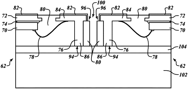
8. A method, comprising:
forming a die pad;
positioning a die on the die pad;
forming a plurality of conductive leads, each of the plurality of conductive leads includes a first portion extending in a first direction and a second portion extending in a second direction transverse to the first direction;
forming encapsulation material on the die pad, the die, and the plurality of conductive leads,
the encapsulation material including a first surface, a second surface opposite to the first surface of the encapsulation material, and a plurality of side surfaces,
the first portion includes a first surface, a second surface opposite to the first surface of the first portion, and a side surface,
the first and second surfaces of the encapsulation material facing in the same directions as the first and second surfaces, respectively, of the first portion,
the encapsulation material being on the second surface of the first portion,
the second portion being spaced from one of the plurality of side surfaces of the encapsulation material in the first direction,
the one of the plurality of side surfaces of the encapsulation material being positioned further away from the die pad in the first direction than the side surface of the first portion; and
forming a conductive layer on the first and side surfaces of the first portion of each of the plurality of conductive leads.
|