| CPC H01J 37/32642 (2013.01) [H01J 37/32174 (2013.01); H01J 37/3255 (2013.01); H01J 37/32568 (2013.01); H01J 37/32715 (2013.01); H01L 21/31116 (2013.01); H01L 21/6833 (2013.01); H01L 21/68735 (2013.01); H01J 2237/334 (2013.01)] | 18 Claims |
|
1. A plasma processing apparatus, comprising:
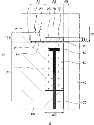
an electrostatic chuck supporting a wafer, and connected to a first power supply;
an edge ring disposed to surround an edge of the electrostatic chuck and formed of a material having a first resistivity value;
a first ring supporting a lower portion of the edge ring, formed of a material having a second resistivity value lower than the first resistivity value, and connected to a second power supply;
an electrode ring disposed in a region overlapping the first ring, in contact with a lower surface of the edge ring, and formed of a semiconductor material having a third resistivity value greater than the first resistivity value;
a first pad only attached to the lower surface of the edge ring and a bottom surface of a stepped portion disposed at an edge of the electrostatic chuck; and
a second pad only attached to a lower surface of the electrode ring and an upper surface of the first ring,
the first ring is surrounding an outer peripheral surface below the stepped portion,
wherein the first resistivity value is a value of 1 S/cm to 10 Ωcm,
wherein the third resistivity value is a value of 90 S/cm to 1000 Ωcm,
wherein a radio frequency (RF) power from the second power supply is applied to the edge ring through the first ring to form an electric field above the edge ring,
wherein each of the first and second pads includes an adhesive material, and
wherein a width of the first ring is the same as a width of the electrode ring.
|