| CPC H01J 37/20 (2013.01) [H01J 37/28 (2013.01); H01J 2237/2007 (2013.01); H01J 2237/202 (2013.01)] | 4 Claims |
|
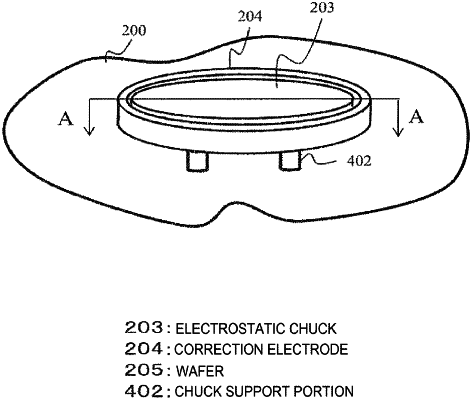
1. A charged particle beam device including an electrostatic chuck mechanism, the charged particle beam device comprising:
a stage which moves a sample, which is to be irradiated with a charged particle beam, relative to an irradiation position of the charged particle beam;
an insulating body which is disposed on the stage and constitutes a dielectric layer of the electrostatic chuck mechanism; and
a ring-shaped electrode which encloses the surroundings of the sample and to which a predetermined voltage is applied;
wherein the ring-shaped electrode is made of a nonmagnetic conductor made of a mixture of aluminum and metal silicon.
|